General description
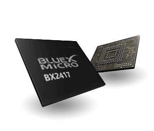
The BX2417 is an ultra-low-power system on-chip(SoC), a Bluetooth chipset, integrated with 32-bit MCU for Bluetooth 5.0 low energy(BLE 5.0) applications which shows the great performance of a leading RF transceiver with low-power consumption. It meets the challenges of a broad range of applications that need advanced Bluetooth LE features.
Also Bluetooth mesh can be run concurrently with Bluetooth LE, enabling smartphones to configure and control mesh nodes.
In this Bluetooth LE device, several digital and analog peripheral interfaces are optimized for external control, including GPIO, UART, IIC, PWM, ADC, and LDOs.
- BLE5.0 supports 1Mbps/2Mbps switch
- Support SIG Mesh
- Meet BQB/SRRC/FCC/CE testing standards
Radio frequency (RF)
- Operating frequency band: 2.4~2.5GHz
- 1Mbps mode reception sensitivity: -93 dBm
- 2Mbps mode reception sensitivity: -90 dBm
- RF output power: -20dBm ~ +8dBm
- 50dB RSSI dynamic range
- The ideal DCDC converter has a receiving current of 3.4mA and transmitting current of 3.5mA at 4.3V
- When the DCDC converter is 4.3V, the receiving current is 4.3mA and the transmitting current is 4.4mA
- When the DC DC converter is 3.3V, the receiving current is 5.5mA and the transmitting current is 5.6mA
Clock and octave
- 32MHz crystal and RC oscillator
- 32KHz RC oscillator
- Support 96 MHZ / 80 MHZ, 64 MHZ / 48 MHZ / 32 MHZ / 16 MHZ clock output
Digital interface
- 11 GPIOs
- 5 channel PWM output
- IO state is maintained during deep sleep
- 2 UART: flow control rate up to 1Mbps, support all baud rates below 1Mbps, support infrared
- 2 I2C: can be master and slave, the maximum speed is 1Mbps
- 2 timers and 1 watchdog
- 1 SPI host: up to 24Mbps
- 1 SPI slave: up to 8Mbps
Analog interface
- 1-way 10-bit AD
- Battery monitoring range: 2.0V~5.0V
- Temperature sensor range: -40°C~85°C
Built-in MCU
- 4-way buffer
- SWD debug interface
- AHB/APB bus clock rate up to 96MHz
Ultra low power consumption
- Sleep current 2.5uA~6uA: SRAM (16~208KB) can be customized
- 1.28 seconds broadcast current: 20uA
Memory cell
- 2Mb Flash
- 208KB OF SRAM is configurable and can be configured independently per 32KB
- 128KB ROM (boot ROM and BLE protocol stack)
- Reserve 32KB of swap memory for BLE connection data
Power management
- Integrated DCDC step-down converter
- 2.3~5.0V voltage input
- One 1.8V LDO 40mA output
- Two 3.3V LDO 50mA and 25mA output each
- Operating temperature: -25℃~85℃
Encryption engine
- ECC
- AES-128
Encapsulation
- QFN 32 pins 4mm X 4mm


